This article was published for the 60th anniversary of Bungard in 01/21
60 Years of Bungard Elektronik
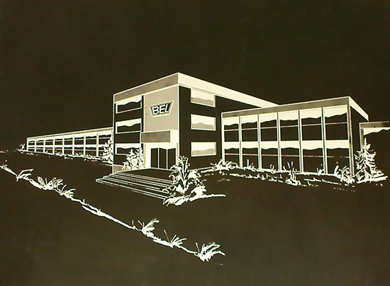


At first glance, all the Bungard equipment looks like a production of printed circuit boards in Legoland format. But on closer inspection, the viewer learns that the manufacturer has made a lot of thoughts when he created a production line in this magnitude.
Those, who want to just quickly realize one or more copies of a specific circuit or make a field test, those fellows will be most certainly customers of the Bungard Elektronik - universities, engineering companies, service providers but also development departments of large production companies – shortly everybody, who designs printed circuit boards. At the beginning of the 60 years company founder Heinz Bungard in Leverkusen considered opportunities for further development in the young industry of printed circuits. It was his idea to equip the copper sheet of a pcb with a UV-light sensitive fotocoat and so he is considered to be one of the inventors of the world-wide-known presensitized PCBs. The Presensitized Base Material is still the major column of the Bungard product portfolio.
In addition, the company has developed into a reliable and important partner as a supplier for the PCB manufacturing companies. When Bungard started production and distribution of the Presensitized Base Material, they were already thinking about supplying small-scale processing equipment for all customers of the Bungard base material.
This market segment was so far totally ignored; e.g. it was impossible to obtain small etching machines or exposure units.
With this idea any manufacturer of designs, prototypes or small series was now capable to produce fast, flexible and above all, error-free PCBs in-house. This was reflected even then in the slogan: "In the morning on the drawing board, at noon already done - with original Bungard Presensitized Base Material”.
The company's founder gave his word with his name and his experience for the quality of original Bungard Presensitized Base Material. Only top quality materials, tested and approved by all usual standards, are used. A broad range of materials such as FR2, CEM1, FR4 and PTFE in various board thicknesses and with different copper clads are offered. From 570 mm x 1150 mm wide boards all standard and special sizes down to a minimum of 50 mm x 50 mm are cut. For the photocoat a high quality positive liquid resist is used, made according to a Bungard owned recipe. The resist features highest exposure sensitivity, short processing turns and large safety tolerances. To paraphrase an advertising slogan: The plates are "indestructible".
With controlled 5 micron layer thickness the resist provides the conditions for rapid and thorough exposure, whereas the optimum of the light source is at 400 nm and the optical resolution less than 30 microns. With the exposure unit Hellas, also in the range of products offered, exposure takes about 90 seconds. After approx. 45 seconds each board can leave the special developer bath at a temperature of 20°C. To protect the photocoat from dust, mechanical damage and unwanted exposure, all materials are covered with a blue foil.
Based on the experience with presensitized PCBs, Heinz Bungard extended his product range. In 1981 he started selling aluminium panels, which were eloxized in a special treatment sequence and then coated with a positive photo resist. Alucorex, so the new product's name, aimed to make manufacturing of front panels, signs, as well as pad printing cliches significantly easier.
Also for the SMT stencils or model components Bungard offers a product that can be processed quickly and economically. These are optional positive or negative photo-coated brass or German silver plates, which can operated in the same machines, with the same chemistry and with no interference of existing internal processes.
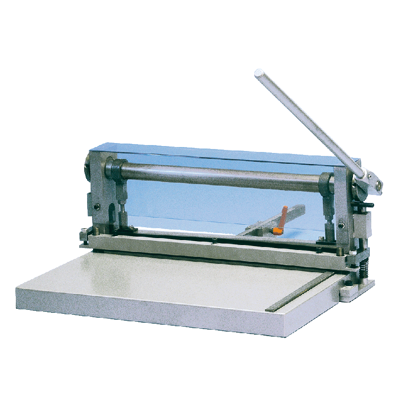
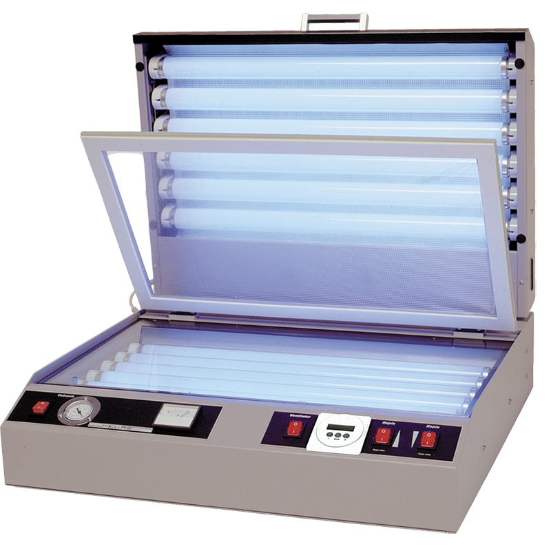
The Bungard had not remained faithful to their line if they did not provide solutions for all major upstream and downstream operations coming up during the pcb-production process. Examples for these solutions are the board cutter NE-Cut (Fig. 1) with a cutting width of 530 mm, the raster photoplotter Filmstar with 8000 dpi resolution, the exposure unit Hellas (Fig. 2) and a parallel light exposure with 8000 Watt power.
Whereas industrial manufacturer cannot see from one end of their etching machine to the other, the Bungard etching machines consist generally of just one unit. The customer can choose between a stationary spray etching machine for either single or double sided boards or a conveyorized spray etching machine. The Splash-Center is a wet processing equipment with static rinse, spray rinse, integrated developer, reserve pool for immersion tin and squeeze dryer.
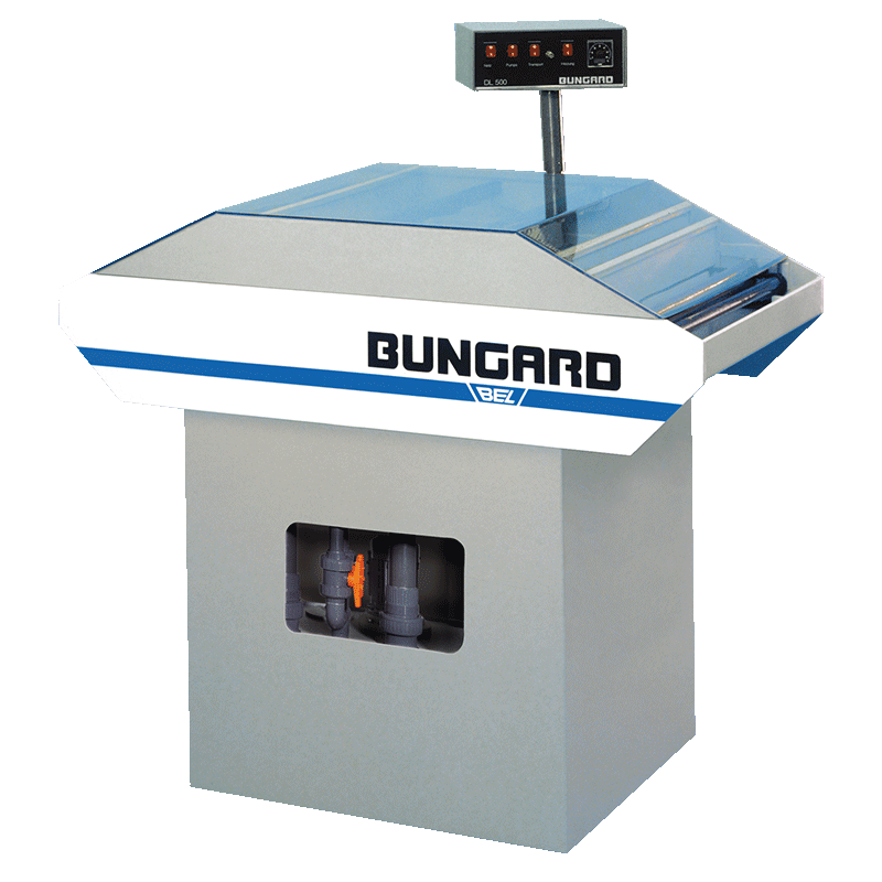
The conveyorized flow system DL 500 (Fig. 3) is on the one side popular for its clean working procedure. Especially in educational environment it is important, that the user can take out clean boards without getting into touch with chemicals. On the other hand the DL 500 achieves more than 5 times the throughput compared to other laboratory etching machines. Thus, small series can be produced easily and quickly.
Whenever you use chemicals a wastewater treatment plant is a useful option. With space requirements of less than half a square meter the wastewater treatment plants fit themselves perfectly into small PCB laboratories. But still the user receives a compact system with a complete closed circuit where nothing is released to the outside, because all substances are taken out of the waste water and demineralized water is flowing back to the machines or the drain.
This is guaranteed by two or three ion exchange columns and, depending on the type, a mineral ph-level-column. The PCB-manufacturer can choose from four models with varying flow rate and absorption capacity.
As an entry level solution Bungard supplies a mechanical through-hole-plating press. Hollow rivets are fitted into the drill holes of a double-sided circuit boards and are then pressed onto the board. Even laboratory manufacturers without any mechanical knowledge will be able to this job. For more complex PCBs and drill holes below 0.6 mm different galvanic plating machines are also available.
Bungard is very proud of their solution for drilling and routing, including developed software. The smallest version offered is the Variodrill system, which can be used for drilling the holes of a PCB. Here, the drilling movement is triggered by a foot switch, same as with a sewing machine. Just step on and off you go! The base material is positioned with both hands under a magnifying glass, while the drill comes from below with a variable speed from 10,000 to 30,000 rpm. A dust extraction system for the drilling dust is included into the delivery.
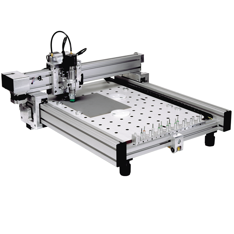
A bit more professional is the CCD/2 drilling and milling machine. The machine drills and routes circuit boards and aluminium front panels and is also suitable for isolation milling. It works with a high frequency spindle, and is also equipped with a depth limiter. Stepper motors control the movement of the x-, y- and z-axis over high precision tooth belts. Boards can be clamped in any position on the machine table, which is equipped with a grid. The user can work with stops and clamping plates or register pins to fix the PCBs or register PCBs and frontpanels for milling at the zero point. If desired, a converter software calculates the milling paths from standard Gerber data.
Really professional you can work with the CCD (Fig. 4). The CCD is designed for direct processing of drill holes, for producing printed circuit boards and machining of surfaces. This machine already looks similar to a professional industry drilling machine which operates in large-scale production. The high frequency spindle goes up to speeds of 60,000 rpm and is stepless adjustable and software controlled. Various data formats can be read in and directly processed with the help of the included driver software for Excellon, Sieb-Meier and HPGL. Thus, a menu-driven processing of individual jobs is possible as well as tool statistics, production utility and Teach-in function. Also, the automatic tool change is inherited from the big professional machines. With a step resolution of 0,00625 mm at approximately 20,000 holes per hour the Bungard CCD can almost compete with its bigger professional sisters.
Brushing machines, laminators, dip coaters, hot air dryers, multilayer press and galvanic through hole plating machines in different sizes and through put round up Bungard company to a full scale supplier for professional prototyping of PCBs. All Bungard machines and Bungard equipment has in common that they use the same technology and apply the same concepts as do industrial machines for large scale production - but just in miniature. A complete, functional lab costs, depending on the desired technology between 15 000 and 40,000 €, but even the "big solution" can be recouped within a year, the company says, if you take into consideration the cost of PCB express service.
After taking over the former competitor Welisch, Bungard was able to establish further production capacities and additional innovation potential in Windeck. In order to fully exploit the associated opportunities, the new BUNGARD Research and Development GmbH was founded in 2014. This increased the floor space by a further 2500 m² and the production and development area by 600 m².
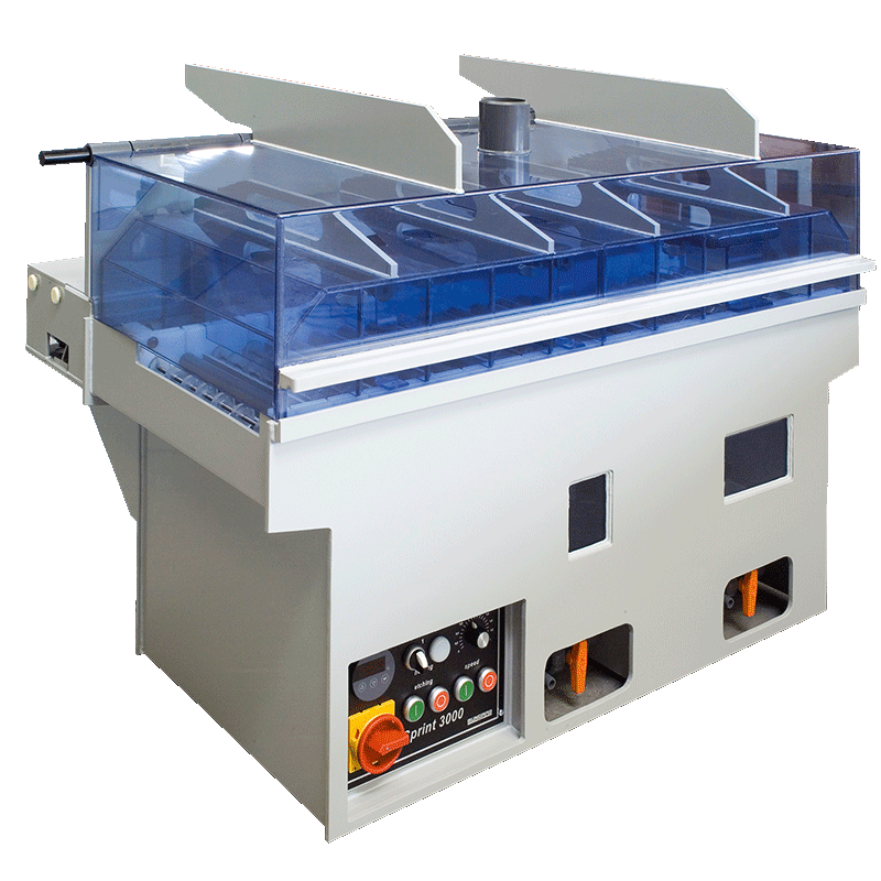
It soon became apparent that this path was the right one. Several new products came onto the market a short time later. A good example of this is the Bungard Sprint 3000 - a newly developed conveyorized spray etching machine for the production of double-sided printed circuit boards with a resolution of less than 0.1 mm.

Rilkestrasse 1
D-51570 Windeck
+49 2292 / 9 28 28 - 29